2018-02-13
 457
457Лабораторная работа №5
Тема: МОДЕЛИРОВАНИЕ ЦИФРОВЫХ УЗЛОВ С ИСПОЛЬЗОВАНИЕМ ПАКЕТОВ МНОГОЗНАЧНОЙ ЛОГИКИ.
Выполнили: группа А-06-15
Дряхлов Иван
Аксенов Алексей
Принял:
Оценка:
Москва,2017
Работа может выполняться с использованием пакетов четырехзначной логики Paket_4 и девятизначной логики STD_LOGIC (файл ieee.vhd в системе моделирования на VHDL для PC).
1. Модифицировать описания схем, полученные в лабораторных работах 2 и 3, с учетом использования четырехзначного алфавита моделирования и средств пакета Paket_4. Включить в VHDL-описание операторы утверждения, контролирующие запрещенные режимы работы узла и ситуации на входе схемы, приводящие к ложному срабатыванию (гонки).
Код Vhdl для четырехзначной логики
PackagePAKET_4is
typeKONTAKTis ('X', '0', '1', 'Z');
Function "not" (A: in KONTAKT) return KONTAKT;
Function "or" (A1, A2: in KONTAKT) return KONTAKT;
endPAKET_4;
Package body PAKET_4 is
Function "not" (A: in KONTAKT) return KONTAKT is
Begin
If A = 'X' then return 'X';
elsif A='1' then return '0';
elsif A='0' then return '1';
else return 'Z';
End if;
End "not";
Function "or" (A1, A2: in KONTAKT) return KONTAKT is
Begin
If (A1='X') or (A2='X') then return 'X';
Elsif ((A1='1') or (A2='1')) then return '1';
Elsif ((A1='0')and(A2='0')) then return '0';
Else return '1';
End if;
End "or";
EndPAKET_4;
Схема сравнения двухразрядных кодов на равенство на элементах ИЛИ-НЕ
library IEEE;
usePAKET_4.all;
entitywer is
generic(T01: time:= 10ns;
T10: time:= 20ns);
port(
a: in KONTAKT;
b: in KONTAKT;
c: in KONTAKT;
d: in KONTAKT;
y: out KONTAKT
);
endwer;
architecturewer of wer is
signal y1: KONTAKT;
begin
process(a,b,c,d)
begin
y1<= not(not(not(not(a)or not(c)) or not(a or c)) or not(not(not(b)or not(d)) or not(b or d)));
case y1 is
when '0' => y<=y1 after T01;
when '1' => y<=y1 after T10;
when others => y<=y1 after T10;
end case;
end process;
endwer;

лаб. 5
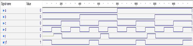
лаб. 2
Графики не имеют явных различий, разве что Yпринимает значение «Х» в начале работы.
Для двухступенчатого JK-триггера с асинхронными RS-входами построить

entity NAND_2 is
port
(x1, x2: in bit; y1: inout bit);
end NAND_2;
entity NAND_3 is
port
(x1, x2, x3: in bit; y1: inout bit);
end NAND_3;
entity NAND_4 is
port
(x1, x2, x3, x4: in bit; y1: inout bit);
end NAND_4;
architecture func_NAND_2 of NAND_2 is
signal s1, s2, s3:bit;
begin
s1<=x1; s2<=x2; s3<=not(x1 and x2);
process(x1, x2, s1, s2, s3);
begin
if((s1’event and s1=’0’)or(s2’event and s2=’0’)) then
y1<=s3 after 1 ns;
elsif((s1’event and s1=’1’)or(s2’event and s2=’1’)) then
y1<=s3 after 3 ns;
end if;
end process;
end func_NAND_2;
architecture func_NAND_3 of NAND_3 is
signal s1, s2, s3, s4:bit;
begin
s1<=x1; s2<=x2; s3<=x3; s4<not(x1 and x2 and x3);
process(x1, x2, x3, s1, s2, s3, s4);
begin
if((s1’event and s1=’0’)or(s2’event and s2=’0’) or(s3’event and s3=’0’)) then
y1<=s4 after 1 ns;
elsif((s1’event and s1=’1’)or(s2’event and s2=’1’) or(s3’event and s3=’1’)) then
y1<=s4 after 3 ns;
end if;
end process;
end func_NAND_3;
architecture func_NAND_4 of NAND_4 is
signal s1, s2, s3, s4, s5:bit;
begin
s1<=x1; s2<=x2; s3<=x3; s4<=x4; s5<=not(x1 and x2 and x3);
process(x1, x2, x3, x4, s1, s2, s3, s4, s5);
begin
if((s1’event and s1=’0’)or(s2’event and s2=’0’) or(s3’event and s3=’0’) or(s4’event and s4=’0’))
then
y1<=s5 after 1 ns;
elsif((s1’event and s1=’1’)or(s2’event and s2=’1’) or(s3’event and s3=’1’))
or(s4’event and s4=’1’)then
y1<=s5 after 3 ns;
end if;
end process;
end func_NAND_4;
entity sch1 is
port
(C, J, K, NS, NR: in bit; Q, NQ:inout bit;)
end sch1;
architecture func_sch1 of sch1 is
component NAND_2 is
port
(x1, x2:in bit; y1:inout bit;)
end component;
architecture func_sch1 of sch1 is
component NAND_3 is
port
(x1, x2, x3:in bit; y1:inout bit;)
end component;
architecture func_sch1 of sch1 is
component NAND_2 is
port
(x1, x2, x3, x4:in bit; y1:inout bit;)
end component;
signal z1, z2, z3, z4, z5, z6:bit;
begin
assert not(NS=’0’ and NR=’0’)
report(“Ошибка! Неопределенное состояние”);
severityerror;
T1: NAND_4 port map(C, J, NR, NQ, z1);
T2: NAND_4 port map(C, K, NS, Q, z2);
T3: NAND_3 port map(z1, NS, z4, z3);
T4: NAND_3 port map(z2, NR, z3, z4);
T5: NAND_2 port map(z3, z1, z5);
T6: NAND_2 port map(z4, z2, z6);
T7: NAND_3 port map(z5, NS, NQ, Q);
T8: NAND_3 port map(z6, NR, Q, NQ);
end func_sch1;
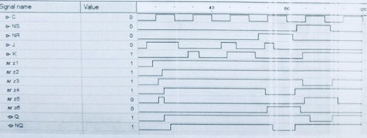
лаб. 5
лаб. 3
Схемы не различаются, так как JK-триггер не имеет запрещенногосостояния.