2015-08-21
 502
502In a semiconductor that indicates electronic conduction in one its part and hole conduction in the other one, the boundary between these two parts is called the electron-hole or p-n junction.
The p-n junction is impossible to obtain by mechanically joining together two semiconductors of different conduction types. To this end, a semiconductor is alloyed with donor and acceptor impurities in such a manner that one part of the semiconductor has electron and the other has hole conduction.
The models of the n-type and p-type semiconductors are given in Fig. 2.6a. The majority carriers-electrons – in the n-type semiconductor are identified with a minus symbol. Ionized donor atoms cannot carry a current as they become a structural component of the n-type semiconductor. They are designated by plus signs in circles. Holes that are also present in the n-type semiconductor are not shown on the model because they are minority carriers here and their density is insignificant against the density of electrons. Similar designations are used for the p-type semiconductor.
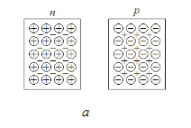
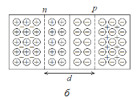
Fig. 2.6. Distribution of charge carriers: a – prior to forming the contact, b –semiconductors in the contact
Assume that the n-type and p-type semiconductors are brought into the ideal contact (Fig. 2.6 b). As the n-region is rich in electrons and the p-region in holes, and vise versa, at the initial moment of contact the density gradient will cause electrons to diffuse from the n-region into the p-region and the holes to diffuse from the p-region into the n-region. An electron that has passed into the p-region is likely to recombine with a hole since the probability of electron-hole recombination is proportional to the density of holes. The same is true of a hole that has escaped into the n-region. In the n-region near the interface between two semiconductors, the donor ions that remain non-compensated in the process will form a positive space charge. In the p-region, it is acceptor ions that are left non-compensated; they set up a negative space charge near the interface.
In the end, the region of transition between the n- and p-type semiconductors will be found depleted of free carriers. This region is called a depletion layer, which just makes for the width of the p-n junction.
The positive space charge of non-compensated donor ions offers opposition to the further diffusion of holes from the p-region to the n-region. The negative space charge of acceptor ions impedes the diffusion of electrons into the p-region, in other words this ions build up at the interface a potential barrier for majority carriers, which can overcome it only if they have sufficient kinetic energies. The system comes to equilibrium as soon as equality is set in the free carrier flows brought about by the carrier density gradient and the space charge field.
If we apply external voltage to a p-n structure with its n-region connected to the positive terminal and the p-region to the negative terminal, then the height of the potential barrier will grow and the current through the p-n junction (neglecting free carrier generation) will be determined by the minority-carrier flow that does not depend on the potential barrier height.
Denote this current by Is. The current flowing through the p-n junction at the given polarity of the applied voltage is called the reverse or back current. With the reversed polarity of applied voltage, the potential barrier to the majority carriers diminishes (Fig. 2.7).
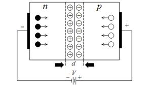
Fig.2.7. Direct voltage applied to p-n junction
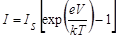
At the external voltage equals to V (considering that voltage drops off across the depletion region), the number of majority carriers that are able to overcome the potential barrier is exp (eV/kT) times grater.
The minority-carrier current remains the same. The total current through the p-n junction may be then expressed by the formula
 ,
,
where k - is Boltzmann’s constant, T – is absolute temperature, e – is electron charge.
At room temperature, kT/e=25 mV. Therefore, at external voltages exceeding 0.1V we may neglect the unity considering that the exponent is equal to no less than e4. The current through the p-n junction may be expressed as
 .
.
This is the forward current in the p-n junction.