2015-08-21
 558
558These transistors have three electrodes: source, from which charge carriers run out; sink, where the charge carriers drain, and gate, which forms the crossed electric field (Fig. 5.1a).
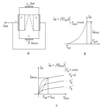
Fig.5.1. Field effect transistor with controlled p-n-junction: a – structure of the transistor, b – sink-gate characteristic, c – set of the output characteristics.
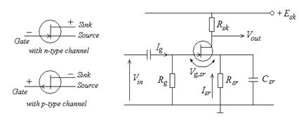
The circuit symbol and the connection diagram with a common source are shown in Fig. 5.2.
The transistor consists of a silicon plate with n-type conduction. This plate is a channel of FET. Two metal conductors are connected to the ends of surface. These two contacts are called a source and sink. The power source Esr and the load resistance Rsr are connected to those conductors (electrodes) in series (Fig. 5.2b). The polarity of the power source provides the motion of majority charge carriers from a source to a sink (they are electrons in a n-type channel). The opposite ends of a plate are alloyed with acceptor impurities which form p-type layers. These two layers are connected to each other and form a common electrode which is called a “ gate ”. Thus, two p-n-junctions are formed (Fig..5.1a).
a b
Fig.5.2. Circuit symbol and application of the FET with controlled p-n-junction: a – circuit symbols, b – circuit diagram of the amplifier
The conduction of a channel is defined by its sectional view. Varying the voltage applied to the gate Vg.sr (Vgate-source), we can change the channel sectional view, and therefore its resistance and the current flowing through it. The voltage Vg.sr has opposite polarity to the polarity of the n-p-junction. When Vg.sr=0 the sink current into the channel has maximum value Isk.max (Fig.5.1b) as the channel sectional view is max. When the reverse voltage Ug.sr increases, the depletion layers of the p-n-junction expands, reducing the sectional view of a channel. At the cutoff voltage Vcut, the channel sectional view comes down to zero and the current Isk tends to zero also. The source and the sink are insulated one from the other. These processes can be illustrated by the sink-gate characteristic Isk=f(Ug.sr), Usk.sr= const (Fig. 5.1b). Fig.5.1c shows the set of sink (output) characteristics Isk=f(Usk.sr), Vg.sr= const. Let’s consider these characteristics when the gate voltage equal to 0 (Vg.sr=0).
When the positive voltage applies to the sink Vsk.sr, the current will increase by non-linear law. The fact of non-linearity can be explained that increasing voltage Vsk.sr leads to decreasing of the channel sectional view the closer to the sink the more. At that, the channel conduction decreases and the current rising becomes slower. When the sink voltage reaches the level of, so-called, the saturation voltage Vsat, the channel near the sink will be closed completely (the channel sectional view near the source remains the same, i.e. V sr=0). Further Vsk.sr rising leads to a little sink current rising, i.e. the resistance of channel increases, and at the same time the sink current reaches the saturation value Isk.max. It is obvious that at Vg.sr=0, Vsat=Vcutoff . The mode of the CVC flat part is called the saturation mode. On the condition that /Vg.sr/>0, the depletion layers spread out and the channel sectional view comes dawn under the action of both voltages Vg.sr and Vsk.sr. The saturation voltage decreases and Vsatt=Vcutoff-Vg.sr for any value of the gate voltage Vg.sr. The voltage Vsat and the saturation sink current Isk.max decrease simultaneously.
The flat parts of output characteristics are used in the operating mode. The high voltage applied to the sink can cause a structure brake down. So, the sink voltage must not exceed the peak value in the operating mode.
Let’s consider the main parameters of FET.
1.The slope of control characteristic describes ability of a device to amplify
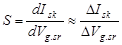 , at
, at  .
.
It has values 0.1-10 mA/V.
2. The inner transistor resistance:
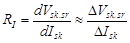 , at
, at  .
.
This parameter changes from hundreds of kilohm to dozens of megohm because the sink current changes little.
3. The input resistance is the differential resistance of p-n-junction biased in a reverse direction.
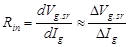 , at .
As for the gate current Ig it is defined by the reverse current of p-n-junction, the input resistance of FET is very high, in the range of 106-109 Ohm.