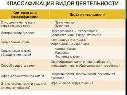
2015-08-21
 476
476FET’s with insulated gate have a metal-dielectric-semiconductor structure. They are called MDS-transistors or MOS-transistors. In the latter, the silicon dioxide (SiO2) is used as a dielectric placed under the gate. There are two types of these devices: with an induced channel and with an embedded channel.
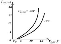
Let’s consider the MDS-transistor with an induced channel of the n-type. If the gate of this device is connected to the source, i.e. Vg.sr.=0, the channel doesn’t exist, and there are two opposing p-n-junctions between the sink and the source (Fig.5.3a). When voltage is applied to the sink, the sink current will be negligible. With negative voltage applied to the gate Vg.sr<0, the layer close to the surface will be enriched by holes. The current in the operation circuit will change a little. If more and more positive bias voltage is applied to the gate Vg.sr>0, the majority carriers of the substrate (holes) will be pushed off the near the surface layer (the depletion layer will expand). At the same time minority carriers (electrons) are attracted by the surface. When the increasing charge exceeds the charge of the rest majority carriers, the type of layer conduction will change. This effect is called inversion of conduction type. With the channel size increase, the sink current reaches the finite value depended on the gate voltage. Further increase is the gate voltage extends the channel and the sink current increases. This is the operating mode of a MDS-transistor. Since the input current is negligible, we get considerable amplification of power. It will be much higher than a BT has.
Thus under the action of an external voltage a conductive channel appears in the FET’s structure. This channel, absent in the equilibrium state, is called an induced channel (induced by the gate electric field). The external voltage which forms a channel, is called threshold voltage (V0, its values are in the range from 1.5 to 10V). FET’s with an induced channel are called the enriched type transistor. The transfer characteristic of such devices is shown in Fig.5.3b.
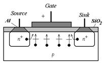
a b
Fig.5.3. Structure of the FET with insulated gate (inducted channel) (a)
and its CVC (b)
There are also MOS transistors with an embedded n- or p-channels placed near the surface layer between the sink and the source. These channels are formed during manufacturing (Fig.5.4). Such devices have channels even if the voltage applied to the gate equals 0. Depending on the polarity of the applied to the gate voltage, the channel can either enlarge (enriched mode) or decrease (depleted mode).
At certain reverse voltage, the charges of the balanced inverse layer are pushed away from the surface by arising cross electric field. The embedded channel becomes depleted, and its resistance increases. This voltage is called the cutoff voltage. FET’s with an embedded channel are called the depleted type transistors.
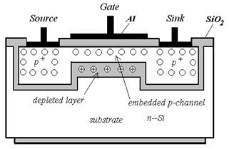
Fig.5.4. Structure of the p-type FET with embedded channel