2018-01-08
 1090
1090Start here
1. Work in small groups. Study the diagrams in Fig. 3.3 and discuss the questions below.
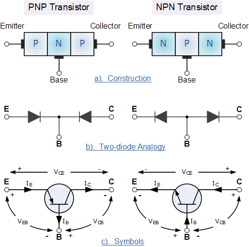
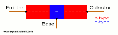
Fig. 3.3. NPN and PNP transistors and their schematic symbols.
1) What types of transistors are depicted in the diagrams?
2) What is their construction?
3) How do you think they work?
4) Why are there diode electronic symbols in Fig. 3.3 b)?
5) What is the difference between these types of transistors?
Listening
2. Listen to the text and decide if the statements below are true or false. Use the diagrams in Fig. 3.3 a) to help you.
There are many different types of transistors. The most basic type is called a bipolar transistor. Bipolar transistors are the easiest to understand. Now let's peer inside a bipolar transistor to see how it works.
Recall that a diode is the simplest kind of semiconductor, made from a single p-n junction, which is simply a junction of two different types of semiconductors, one that's missing a few electrons and thus has a positive charge (p-type semiconductor) and the other with a few extra electrons, thus having a negative charge (n-type semiconductor).
By itself, a p-n junction works as a one-way gate for current. In other words, a p-n junction allows current to flow in one direction but not the other. A diode is simply a p-n junction with a lead attached to both ends.
A transistor is like a diode with a third layer of either p-type or n-type semiconductors on one end. Thus, a transistor has three regions rather than two. The interface between each of the regions forms a p-n junction. So another way to think of a transistor is as a semiconductor with two p-n junctions.
One way to make a transistor is with a p-type semiconductor sandwiched between two n-type semiconductors. This type of transistor is called an NPN transistor because it has three regions: n-type, p-type, and n-type.
The other way to make a transistor is just the opposite, with an n-type semiconductor sandwiched between two p-type semiconductors. This type is called a PNP transistor because its three regions are p-type, n-type, and p-type.
Each of the three regions of semiconductor material in a transistor has a lead attached to it, and each of these leads is given a name: collector, emitter, and base.
1) The most basic type of transistors is a bipolar transistor.
2) A diode is made from two p-n junctions.
3) P-type semiconductor is missing a few electrons and thus has a negative charge.
4) N-type semiconductor with a few extra electrons, thus having a positive charge.
5) A diode is the simplest type of semiconductor.
6) A p-n junction works as a one-way gate for current.
7) A transistor is a single p-n junction.
8) There are two types of bipolar transistors: a P-N-P transistor and an N-P-N transistor.
9) The leads of a transistor are called emitter, collector and base.
Vocabulary
3. Complete the sentences, using the diagrams in Fig. 3.3 to help you.
· In an NPN transistor, the (1) …………is the positive side of the transistor. The (2) ………… and (3) ……….. are the negative sides.
· In a PNP transistor, the base is the (4) ………..side of the transistor. The collector and emitter are the (5) …………..sides.
· The (6) …………. and the (7)…………are attached to the largest of the semiconductor regions.
· When voltage is applied to the (8) ………., current is allowed to flow through the collector to the emitter.
· The (9) ……….. is attached to the middle semiconductor region.
· The (10) ………. serves as the gatekeeper that determines how much current is allowed to flow through the collector-emitter circuit.
Task
4. Use the symbols Vce, Vbe, Ice, Ibe in Fig.3.3 c) to complete the sentences.
These two current paths are important in a transistor:
Collector-emitter: The main current that flows through the transistor. Voltage placed across the collector and emitter is often referred to as (1) ….., and current flowing through the collector-emitter path is called (2) …...
Base-emitter: The current path that controls the flow of current through the collector-emitter path. Voltage across the base-emitter path is referred to as (3) ….. and is also sometimes called bias voltage. Current through the base-emitter path is called (4) …..
Reading
5. Read the text below. Match the descriptions 1-2 with the diagrams in Fig. 3.4. Put the descriptions in logical order. Indicate the n-type and p-type regions, holes and electrons. Entitle the points a) and b) in Fig. 3.4.
 a)
a)
 b)
b)
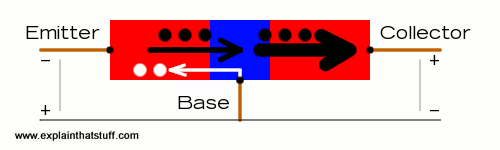
Fig. 3.4 How an NPN transistor works.
1) A transistor works when the electrons and the holes start moving across the two junctions between the n-type and p-type silicon. Let's connect the transistor up to some power. Suppose we attach a small positive voltage to the base, make the emitter negatively charged, and make the collector positively charged. Electrons are pulled from the emitter into the base – and then from the base into the collector. And the transistor switches to its "on" state.
2) When no current is flowing in the transistor, we know the p-type silicon is short of electrons (shown here by the little plus signs, representing positive charges) and the two pieces of n-type silicon have extra electrons (shown by the little minus signs, representing negative charges). Another way of looking at this is to say that while the n-type has a surplus of electrons, the p-type has holes where electrons should be. Normally, the holes in the base act like a barrier, preventing any significant current to flow from the emitter to the collector and the transistor is in its "off" state.
6. Put the sentences A-H in logical sequence order 1-8.
1) …. 2) …. 3) …. 4) …. 5) …. 6) …. 7) …. 8) ….
A. Turn on the base current and a big current flows.
B. Technically, this type of transistor is called bipolar.
C. So the base current switches the whole transistor on and off.
D. But it also acts like a switch at the same time.
E. The small current that we turn on at the base makes a big current flow between the emitter and the collector.
F. Because two different kinds (or "polarities") of electrical charge (negative electrons and positive holes) are involved in making the current flow.
G. When there is no current to the base, little or no current flows between the collector and the emitter.
H. By turning a small input current into a large output current, the transistor acts like an amplifier.
7. Read the following paragraph. Work in pairs. Create tasks, such as filling in the gaps, for your fellow students to do.
We can also understand a transistor by thinking of it like a pair of diodes. With the base positive and the emitter negative, the base-emitter junction is like a forward-biased diode, with electrons moving in one direction across the junction (from left to right in Fig. 3.4) and holes going the opposite way (from right to left). The base-collector junction is like a reverse-biased diode. The positive voltage of the collector pulls most of the electrons through and into the outside circuit (though some electrons do recombine with holes in the base).
Speaking
8. Explain how a field-effect transistor (FET) works. Use the diagrams in Fig. 3.5 and the information in the previous tasks to help you. Exercise the following words and word combinations:
· Field-Effect Transistor (FET);
· controlling the movement electrons;
· gate, source, drain;
· Metal Oxide Semiconductor Field-Effect Transistor (MOSFET)
· extra electrons in the n-type source and drain
· holes in the p-type gate
· a positive voltage, an electric field
· switch the transistor on and off
· a unipolar transistor
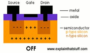
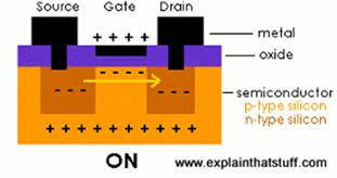
Fig.3.5. How a field-effect transistor (FET) works.
9. Work in pairs. Make dialogues about the difference between a bipolar and a field-effect transistor.
Writing
10. Make a comparative table of a bipolar and a field-effect transistor.