2015-08-21
 490
490The matter is that intrinsic semiconductors are used rarely in electronics. Extrinsic semiconductors are widely used for production of active semiconductors. This is determined by the possibility to get carriers of both charges (electrons and holes) and to control their density with high accuracy.
Free electrons and holes appear simultaneously when a covalent bond is being broken. If it was possible to get a free electron without breaking (disrupt) a covalent bond, the holes would not appear and we could get the free electron density exceeding the holes one. In the same way, if it was possible to get a broken covalent bond without a free electron, the holes density would be higher than that of the free electrons. This will be possible if a semiconductor is alloyed with a small number of foreign elements which are called impurities.
Every germanium or silicon atom from the crystal lattice has four valence electrons, which take part in formation of covalent bonds. If germanium or silicon is doped with an element having five valence electrons, we get one extra electron. The fifth valence electron does not take part in covalent bonding and can be mobile and free without breaking covalent bonding, i.e. without forming a hole. When the fifth electron becomes free, the crystal lattice will have a positive charge ion (as metals have). Impurity that has more valence electrons than necessary to build up the bonds between the neighboring atoms of the host material is known as a donor, and a semiconductor doped with such impurity is called a semiconductor with electronic or n-type conduction. Elements with 5 valence electrons locate in the V group of the Periodic Table. Silicon or germanium is usually doped with such elements as phosphorus, arsenic or antimony.
The n-type semiconductor contains free electrons, acquired from a donor impurity and also have several broken covalent bonds. Each of broken covalent bonds forms free electrons and holes. Thus, there are two types of mobile charge carriers, but now the number of free electrons exceeds the number of holes. That is why electrons in the n-type semiconductor are called majority charge carriers, and holes are minority.
If a semiconductor is alloyed with an impurity element belonging to Group III of the Periodic Table, then all 3 valence electrons of the impurity atom will be needed to form a complete covalent bond structure. So, we get a broken covalent bond without a free electron. Thus, it is possible to increase the number of holes beside the number of free electrons. The impurity atom is electrically neutral, but if its 3 valence electrons are distant from a positive hole, it becomes an unmoved negative ion in general.
Actually, the impurity atom captures an electron to complete the covalent bond between two atoms (neighboring and host substance). That is why such impurity atom is called an acceptor. In this case the majority charge carriers are holes, and electrons are minority carriers. A semiconductor with such an impurity is called a semiconductor with p-type conduction. The elements with 3 valence electrons are placed in the third group of Mendeleev’s table. Boron, aluminum, gallium or indium can be used as impurity with germanium or silicon.
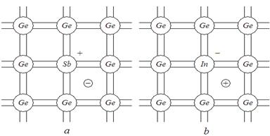
Fig. 2.3. Germanium (Ge) crystal with impurities: a – donor impurity (antimony Sb), b - acceptor impurity (indium In)
Let’s evaluate the number of impurity atoms necessary to change the density (concentration) of electrons or holes. Let’s suppose, for example, that it is necessary to get n-type silicon with 1015 free electrons per 1cm3. Since, at room temperature a pure silicon contains only 1010 free electrons per 1cm3 and additional electrons it can get only from a donor impurity, i.e. it is necessary to add 10  donor atoms into each 1 cm
  of silicon. Each atom of silicon contains
  atoms. So, it is enough to add only one impurity atom for every 50 million atoms of silicon to get 1015 free electrons per 1cm3. If we have phosphor as impurity whose atomic mass is about silicon’s one, it will be enough to add only 20 milligrams of phosphor per 1 kg of melted silicon. This tiny dope of impurity increases the number of free electrons in five-power. This is the evidence that germanium and silicon must be cleared with a high accuracy before being used in semiconductor devices. The permissible limit of a foreign impurity is not more than 10-8 % for Ge, i.e. not more than one atom per 10 milliard atoms of Ge, it is less for silicon – 10-11 %.
The semiconductor’s dopant has influence on the density of minority carriers. It comes down as much as the majority carriers density grows.