2015-08-21
 624
624Many materials with a large range of thermal, mechanical and electrical properties are widely used in electronic engineering. The electrical conduction is the most important physical property of a material for construction of electronic devices. With reference to conduction materials are divided into metals, insulators and semiconductors. Electrical conduction is the ability to conduct electrical current under applied voltage. Such metals as copper, silver and aluminium are excellent conductors, whereas such insulators as diamond and glass are very poor conductors. At low temperature pure semiconductors behave like insulators. Under high temperature or light or with impurities, however, the conduction of semiconductors can be increased considerably, reaching the levels that may approach those of metals.
Metals differ from insulators by a number of free charge carriers which are in the empty conduction band. Electrons of a solid-state body are situated in strictly definite energy levels, although, the number of energy levels is unlimited. Those electrons, which are closer to the nucleus, have less energy and are situated in lower energy levels. It is necessary to surmount the mutual attraction to set an electron apart from a nucleus, in other words, it is necessary to spend some energy. When an electron changes its location from a higher energy level to a lower one, some energy is given off. It is called quantum of energy. If an atom absorbs quantum of energy, the electron will change its location from a low energy level to a higher one.
According to the band theory energy levels form so-called allowed bands. The upper allowed band at the temperature of absolute zero (T=0K) is empty or partly filled with electrons. This band is called the conduction or empty band. The next allowed band is called the valence band. At the temperature (T=0K) it is completely filled with electrons. Only electrons from the valence band can be involved in chemical and electrical processes. Just these electrons can reach some energy levels in the outer atom shell.
Lower energy levels form other full of electrons bands, but they are hardly ever involved in a phenomenon of electroconduction. That is why we’ll skip their consideration.
Metals have a lot of electrons which are situated above the valence band in higher energy levels. These levels form an empty band or the band of conduction. Electrons occupying this band are called conduction electrons. They move without any order and jump from one atom to another. Just these electrons provide high conduction of metals.
At room temperature (T=300K), conductors have the conductivity 104-106 Sm/cm (Sm/cm – conductivity of 1 cm  ).
).
The structure of metal energy bands is shown on Fig. 2.1a.
The lateral lines image the energy levels of electrons. The distance between the energy levels does not exceed 10-17 eV. But since the electrons energy at room temperature comes to 0.03 eV, electrons can freely move inside a band from one level to another one.
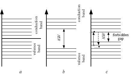 Fig. 2.1. Diagrams of energy levels in: a – metals, b – insulators,
c – semiconductors
In metals the completely empty conduction band and the completely full valence band lie next to each other (Fig. 2.1 a), and they form a combined band in which the number of energy states exceeds the number of electrons. Thus, at normal temperature, a great number of electrons have enough energy to move from the valence band to the conduction one. These electrons can carry an electric current. This fact explains why metals have high conductivity. Practically, every atom of metal gives the conduction band at least one electron. So, the number of conduction electrons isn’t less than the number of atoms (5.1022 free electrons in 1cm3). Adjacent atoms of metals interact in such a way that they form a crystal lattice and are bonded by forces of interaction. But under applied electric field outer electrons and valence electrons of each atom become free and get a possibility to move in the structure. The rest of electrons and nuclei stay strictly fixed in their points of a crystal lattice.
Each atom is electrically neutral, so the entire structure is also electrically neutral. When a valence electron separates from an atom, the rest of electrons and a nucleus are bonded by a crystal lattice, and we can consider itas a positive ion. As far as bonded positive ions are distributed uniformly in the crystal structure, moving electrons are also distributed uniformly. Hereby, we have such model in metals: bonded positive charged ions are surrounded with a homogeneous “gas” of moving electrons. Therefore, positively charged atoms don’t take part in the process of conduction because they are fixed. Only free electrons are current carriers in metals. The density of these electrons depends on the number of valence electrons in the atom and is constant for each metal.
The structure of insulator energy bands (Fig.2.1 b) is quite different from that of metals. Insulators have a very wide energy region between empty and filled bands. It is called the forbidden energy gap. The energy gap contains energy levels where electrons can’t be located. The width of the forbidden gap  is at least several electron-volts. At normal temperature, only a few electrons are located in a conduction band. The electrons from a valence band can not overcome a wide energy gap, and they can not reach a conduction band. Thus, insulators are bad conductors, but at higher temperatures, having acquired external energy, valence electrons can move to a conduction band. At T=300K insulators have electrical conductivity less than 10-10 Sm/cm.
The semiconductor band diagram is similar to that of an insulator (Fig.2.1 c), but its forbidden gap width is less than in an insulator. It is about 1 eV. Thus, at a low temperature, semiconductors behave as insulators, but under normal temperature, a great number of electrons may jump into the conduction band and enhance electric conductivity. At T=300K, it is within 10-10 – 104 Sm/cm.
The most frequently used materials in semiconductor technology are germanium (Ge) and silicon (Si) although other semiconductor materials may be used. Their outer atom shells have four valence electrons. The crystal lattice of semiconductors consists of atoms bonded by valence electrons. Such bond is called a covalent bond (Fig. 2.2 a).
Similar to metals, pure semiconductors have regular geometrical figures which form a crystal lattice, but most of valence electrons can not move freely in a crystal. They are bonded by a covalent bond with atoms, which are strictly fixed in the nodal points of a crystal lattice. At T=0K all valence electrons are involved in this bond, and there are no free carriers for conduction in a crystal. However, heating of a semiconductor increases oscillations of the atoms near the equilibrium state in a crystal lattice. Having acquired kinetic energy from an external source, some valence electrons brake a covalent bonding (interatomic bonding forces) and begin moving at random inside the crystal lattice. Thus, they form a “gas” of moving electrons. These electrons may by called the conduction (band) electrons.
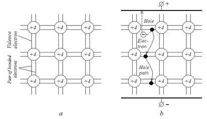
Fig.2.2. Germanium crystal lattice (a) and hole current in it (b)
When a covalent bonding is broken (disrupted) and the electron escapes, the atom itself acquires a positive charge equal to the electron charge. The positive charge, produced due to the loss of one electron, is called a hole. Such atom state is non-stable since an electron from the adjoining atom may jump into this hole and the hole will become filled, i.e., the positive charge will be neutralized and the crystal will stay electrically neutral. As a result, holes are capable to move as positive charges.
The electrons filling the holes are called substitution electrons. Under the action of the external electric field the holes will move (as a positive charge) in the direction of force lines, i.e. from the positive to the negative terminal of the supply source. The motion of the holes forms a hole current.
Thus, the current flowing through a semiconductor will be the sum of electron and hole currents. This fact explains the main difference between currents flowing through a semiconductor and a metal. Keep in mind that:
1. Both currents in a semiconductor are essentially electron cur
rents because the hole current is the motion of substitution
electrons in the same direction as conduction electrons move.
2. Holes have less mobility because they move from atom to atom rather than directly between the source terminals. As a result, the hole current forms a less portion than the electron current in the total current flowing through a semiconductor.
The number of free electrons in a pure semiconductor is equal to that of holes. In a semiconductor charge carriers, i.e. electrons and holes, appear in pairs, and the process is know as the generation of electron-hole pairs. Such process can start under the action of heat, electric field, light, and imported impurities also.
Pair generation is accompanied with recombination of carrier pairs into neutral atoms. Electrons from the conduction band jump to the valence band and occupy free energy levels which correspond to holes. Herewith, electrons and holes disappear as free carriers of charge (electron acquires bonded position).
These processes compensate each other and we have equilibrium state. The concentration (density) of electrons is equal to the density of holes.

where n – concentration of electrons, p – concentration of holes.
For germanium at room temperature n1=p1=1013 per cubic centimeter, for silicon - 1010.
Semiconductors, like metals, have the same number of atoms in 1 cm of material (5.1022), so semiconductors have much less charge carriers than metals have free electrons. For example, resistance of copper at room temperature is 0.017.10-4 Ohm.cm, but germanium has 50 Ohm.cm, silicon has 10.104 Ohm.cm. The width of the forbidden gap is 0.75 eV for Ge and 1.12 eV for Si.