2015-08-21
 564
564Bipolar transistor (BT) is designed for amplification and generation of oscillations. The principle of operation of a BT employing one of its basic circuit connections may be laid down (or formulated) as follows: when an alternating current of a definite value feeds small input resistance of the BT simultaneously at its output a current of approximately the same value feeds a large load resistance, thus providing power amplification. The transfer of a small input resistance to a large load resistance occurring in such a transistor gave it the name ‘TRANsfer reSISTOR’, abbreviated transistor. The transistor basically consists of a germanium or silicon crystal and two p-n-junctions. In essence, the BT is made up of two diodes connected back to back. As shown in Fig.4.1, a transistor crystal has three regions: the left-hand hole region (p-region) called the emitter, the middle electron region (n-region) known as the base and the right-hand hole region (p-region) called the collector of electrons. The BT's having such a structure are known as the P-N-P type transistors and are widely used in electronics.
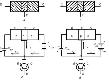
Fig. 4.1. Transistor types: a - P-N-P transistor, b – N-P-N transistor, c – supply of P-N-P transistor and its circuit symbol, d - supply of N-P-N transistor and its circuit symbol
There are also transistors in which the p-region is between two n-regions as shown in Fig.4.1b. Transistors of such a structure are called the N-P-N type transistors. The majority carriers in the N-P-N transistor are electrons.
Since the emitter of a transistor serves as a source of charge carriers the emitter regions should have the highest concentration of its own majority carriers, which is achieved by appropriate doping it with impurities. The concentration of charge carriers in the collector region is less than in the emitter region since it receives, so to say, ‘foreign’ carriers (analogous to the anode in an electron valve). The base region has the lowest concentration of its own majority carriers as it controls the motion of ‘foreign’ carriers (analogous to the control grid in an electron valve). Each region is provided with a metal terminal (a lead).
Let us now connect DC voltage sources between the emitter and base terminals, VEB, and the collector and base terminals, VBC, observing the following rule: a low emitter-to-base voltage (a fraction of a volt in low-power transistors) and a collector-to-base voltage (volts, sometimes over a dozen of volts) must be forward and reverse (cutoff) voltages, respectively.
Fig. 4.1c illustrates the supply sources for the P-N-P type transistor. Note that the negative and positive terminals of the corresponding butteries are connected to the collector and emitter, respectively, so that the current flow (motion of positive charges) is directed from the emitter to the base. It is motion that is indicated by the arrow in the circuit symbol of the p-n-p type transistor shown in the same figure. The supply sources for the n-p-n type transistor shown in Fig. 4.1d are connected in compliance with the same requirements for the transistor junctions, i.e. the collector circuit is connected here to the battery positive terminal. Current flow (opposite in direction to electron flow) is directed from the base to the emitter and the reverse direction of the emitter arrow permits the n-p-n transistor to be distinguished from the p-n-p transistor in schematic diagrams.
Let’s consider the directions and relationships between the currents in the connecting wires (Fig. 4.1c).
The holes pushed away from the left p-region by the positive voltage VEB diffuse through the left hand junction (low potential barrier) and move into the n-region of the base (in forward direction). The holes partly recombine here with base electrons. The base region is made, however, extremely thin (fraction of millimeter, this is very important) and, therefore, the great majority of holes (up to 99%) reach the right-hand junction by diffusion. The holes (being here the minority carriers) pass freely through the right-hand junction and after drifting through the right p-region are attracted by the negative voltage VCB, thus producing the current Ic in the collector circuit. The charges carried by holes from the left p-region are replenished by the current IE flowing in the emitter circuit through the voltage source VEB. Finally, the base region electrons recombining with emitter holes are supplied from the external circuit, thus producing the base current IB. The base current is approximately the difference of emitter and collector currents as follows from the process discussed above i.e.,
IB = IE - IC..
In the circuit diagram shown in Fig. 4.1d the formation of currents is similar to that described above, with the difference that electrons, not holes, move to the right from the emitter, and current in the circuits flows in reverse directions. Therefore, the processes occurring in the n-p-n type transistor are self-evident.
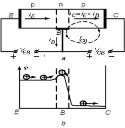
Fig. 4.2. Process in P-N-P transistor: a - currents; b - hole flow
Let us discuss in some detail the physical processes occurring in the p-n-p type transistor (Fig.4.2a). If the emitter circuit is open, then the current flowing from the collector through the base will not disappear completely. While approaching the right p-n junction, the conduction electrons from the right p-region move into the n-region and produce the current IC0 shown by the dashed line in Fig.4.2a. In the collector circuit the direction of this current coincides with that of the main current IC, whereas in the base circuit the current IC0 is opposite to the main current IB, thus the base current is the difference of these two currents. The current IC0 is known as the collector cutoff current. It is rather low as it is produced by minority carriers of the right p-region. The base current IB is generally higher than IC0 and its direction is determined by the holes moving from the base region. However, the current IC0 must be taken into account since it rises abruptly with temperature (approximately doubles for each 10ºC). This should be considered when providing temperature stability of transistor equipment.
Let us trace the main path of majority carriers (holes) in the p-n-p type transistor as shown in Fig. 4.2b. The holes move from the emitter through the emitter junction (whose potential barrier is reduced by the voltage VEB) and then through the collector junction (whose electric field permits minority carriers to pass freely), and finally the holes are attracted to the negative collector electrode.
This process is remarkable by the following: the value of collector current is determined by the flow of holes through the left junction, i.e. by the voltage VEB, since only several and even a fraction of a percent of the over-all amount of holes are branched off into the base circuit, whereas field intensity at the right junction is always sufficient to attract holes into the collector region, and therefore voltage at the collector has practically no effect on collector current. The last property is similar to the influence of anode voltage on anode current in a pentod.
Let us discuss a simple (but not always the last) transistor circuit similar to those shown in Fig.4.2.
Which may be referred to as a common-base configuration since the base terminal is the common (grounded) point for all three electrodes. Such a circuit is given in Fig.4.3.
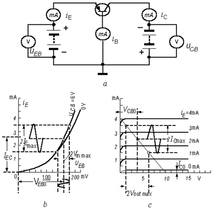
Fig. 4.3. Common-base transistor: a - schematic diagram; b - input characteristics; c – output characteristics
All circuit characteristic curves may be taken by connecting the instruments (gages) as shown in the figure and measuring the currents as steps change the voltages. The emitter circuit is called the input circuit, as a signal source will be connected into it. The collector circuit is called the output circuit since a load will be connected to it. Relationships  and
and  are called respectively input and output characteristics of a common-base transistor.
The input characteristic (Fig. 4-3b) being the relationship between emitter current and input (emitter-to-base) voltage for a constant collector-to-base voltage is similar to the characteristic curve of a forward-biased crystal diode since a forward biasing voltage is applied to the left p-n junction.
If VCB = 0, i.e. if the collector is shorted to the base, we obtain precisely the diode characteristic curve.
Passing through the origin of coordinates. When VCB is increased, the input characteristic is shifted slightly upwards since the collector voltage, as already stated above, has practically no effect on the emitter junction. For this reason, only one input characteristic is sometimes given in manuals for a common-base transistor.
Let us examine output characteristic curves (Fig. 4.3c) proceeding from the lowest one corresponding to iE = 0, i.e. when the emitter circuit is open. This is characteristic curve for the collector cutoff current ICO; it runs from the origin of coordinates and represents a current flowing through the diode in the reverse direction. At normal temperatures collector cutoff current in receiver transistors amounts to several microamperes. The curves located above the collector cutoff current characteristic curve represent a family of constant emitter current. As is known, collector current is proportional and almost equal to emitter current (except for a small fraction of charge carriers “intercepted by the base»). Therefore, the characteristic curves are linear, nearly horizontal and equally spaced one from another. The slight rise of the nearly horizontal portions of the characteristic curves is caused by a spread of the right-hand junction with growth of the cutoff voltage VCB and, consequently, the reduced base thickness leading to a smaller percentage of charge carriers, which manage to recombine in the base region. Note that plotting the voltage VCB to the right we do not indicate its negative sign, this, however, should be remembered when dealing with p-n-p transistor.
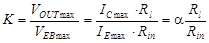
What advantages and disadvantages does the common-base circuit have? Let us connect a source of signal voltage VEBmax (Fig.4.4) with the amplitude Vin into the input circuit after selecting the initial positive bias VEbo, so as tooperate on the linear portion of the input characteristic curve (thus, eliminating nonlinear distortions). Under these conditions an AC component with amplitude IEmax appears in the emitter circuit. With input voltage equal to several millivolts this current will prove to be equal to several milliamperes. This indicates the high input conductivity of the common-base circuit. In other words, the input resistance Rin amounts to only dozens of ohms.
Let us connect a load resistor Rl into the collector circuit of the diagram shown in Fig. 4.4 and assume the signal voltage across Rl and the power in it to be useful output of a common-base transistor amplifier. Remember that flat output characteristic curves indicate a high output resistance Rout of the semiconductor device. This is quite natural since the collector junction with reverse bias has a really high resistance (dozens and hundreds of thousands of ohms). Therefore the resistor Rl may be chosen to be more than 1KΩ, provided the DC voltage drop across the collector is permissible. In Fig.4.3c the line of load is shown at the angle Q corresponding to Rl = 2500Ω with battery voltage ECB = 10V. The amplitude of alternating collector current Icmax will be apparently almost equal to that of the emitter current IEmax. This may be expressed more precisely in the formula:
 ,
,  .
.
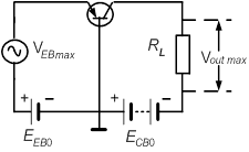
Fig. 4.4. Common-base transistor amplifier with a load resistor
Where α<1 is that portion of charge carriers which moves from the emitter through the base and reaches the collector. The parameter α is defined as the emitter-to-collector current gain of a common-base transistor or simply the common-base current gain. The value of α may vary from 0.95 (for the worst transistors) to 0.998 (for the best transistors). For practical purposes, α is generally rounded off to unity (α=1). Voltage gain in the common-base transistor amplifier will be evidently more than unity, if the output current nearly equals the input current and the load resistance exceeds the input resistance, i.e.
 .
.
Thus we have explained physically and determined quantitatively signal voltage amplification in the common-base transistor amplifier. If we assume, for instance, that α = 0.98, Rin = 50Ω and Rl = 2500 Ω, then the voltage gain will be K=0.98 (2500/50) = 50.
Power gain Kp will prove to be nearly the same as the voltage gain since
 .
.
Now the common-base transistor amplifier may be characterized rather fully. It has a very low input resistance and a high output resistance. This means that it is suitable for applications where the signal source has a low internal resistance and load resistance can be chosen sufficiently high - hundred or a few hundreds of ohms.
The current gain was proved to be less than unity (Kcur =α) and the power gain was equal roughly to the voltage gain. The output characteristic curves of the common base transistor amplifier are flat and parallel to each other, thus providing operation without linear distortions.
The transistor may also employ another circuit connection, which permits signal voltage and current to be amplified. This circuit configuration is termed a common-emitter circuit (Fig.4.5).
The common-emitter connection of a transistor is similar to the connection of a vacuum triode. In fact, the emitter, base and collector are connected in much the same way as the triode cathode, grid and anode, respectively. The signal source having the voltage VBEmax is connected into the base circuit in addition to the initial bias source EBE0. The load (for instance, the resistor RE) is connected into the collector circuit in series with the supply source ECF. Let us consider the characteristic curves of the common-emitter transistor under static conditions, i.e. when the terminals of the signal source and the resistor RE are shorted. The input characteristic relates base current to base-to-emitter voltage for a constant collector-to-emitter (output) voltage. In low-power transistors base current amounts to a fraction of a milliampere. The characteristic curve corresponding to V CE = 0 (collector and transistor are shorted) is similar to the characteristic curve of a forward-biased crystal diode. If now voltage VCE is turned on, the base current of a new characteristic curve will decrease at the same voltages across the base since the collector will intercept charge carriers moving from the base region. With a small voltage applied to the base, base current even reverses its direction. This is explained by the fact that the collector cutoff current flowing through the base wire in the opposite direction to the base current becomes dominant in the base circuit.
With further increasing the voltage VCE the input characteristic curve is shifted only slightly. Therefore, we may limit ourselves to a signal input characteristic curve taken at a normal collector voltage. The right-hand curve taken at VCE =5V may serve as such a characteristic curve in the example shown in Fig.4.5b.
The output characteristic of the common-emitter transistor relates collector current to collector to emitter voltage for a constant base current. The lower curve in the family of output characteristics shown in Fig. 4.5c corresponds to iB = 0 which means that the base circuit is open. Under these conditions open-base emitter current ICE0 (of about hundreds of microamperes for receiver transistors) flows from the emitter to the collector. This current is greater than conventional diode reverse current since collector-to-emitter voltage drops partially across the emitter junction in the forward direction.
When iB > 0, the output characteristic curve runs above the one for iB = 0 (Fig.4.5c). In fact, when base current is increased, the emitter current (being many times the base current) also increases. Simultaneously, the collector current increases with emitter current. On the operating portion of the output characteristic curve collector current will somewhat increase as the voltage VCE is increased and the current iB is hold constant. In fact, if the voltage across the collector junction is increased, the base thickness is reduced, thus the base current will go down. But the output characteristics are plotted for iB =constant, and one has to raise the bias voltage EBE so as to maintain the base and emitter currents constant.
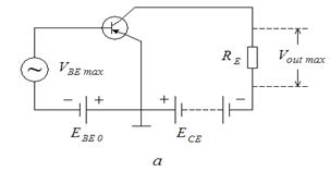
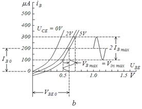
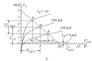
Figure 4.5. Common-emitter transistor: a – transistor amplifier with a load resistor, b – input characteristic curves, c - output characteristic curves
When the base current is given a next step rise, a new characteristic curve running above and parallel to the previous characteristic is obtained. Their operating portions are steeper than those of output characteristics for the common-base transistor Fig.4.3c. This is an indication that the output resistance of the common-base transistor. It amounts generally to thousands or several dozen of thousands of ohms. However, the input resistance of the common-emitter transistor is hundreds and even higher than a thousand ohms as can be seen from Fig.4.5b. It is by these parameters that the common-emitter circuit is distinguished basically from the common-base circuit.
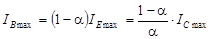
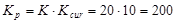
Before considering the amplifying properties of the common-emitter transistor, attention should be given to the initial portions of its output characteristic curves. As collector-to-emitter voltage VCE drops down to zero (with the base circuit being closed), collector current sharply falls to zero and then starts to flow in the reverse direction. The fact is that the forward bias voltage supplied to the collector junction becomes dominant under these conditions. Collector reverse current is practically zero when a transistor operates as an amplifier and therefore, the fact of current cutoff (and the value of cutoff voltage at the collector) becomes of great importance. Let us consider the amplifying properties of the common-emitter circuit (Fig.4.5a) capable of amplifying the signal current. In fact, if the load resistance were zero (the output terminals short circuited), the collector alternating current ICmax would amount to the fraction α of the emitter alternating current IEmax.
At the same time the input signal current is the base current which, as we know, amounts to the fraction (1- α) of the emitter current.
Consequently,
 .
.
Hence, with the output terminals short-circuited the current gain will be:
 .
.
The parameter b is defined as the current gain of the common-emitter transistor. In fact, current is amplified in this circuit since b > 1. If, for instance, a = 0.98, then b = 0.98 / (1-0.98) = 49. Current amplification can be explained quite easily, namely, in the common-emitter circuit the signal controls a great collector current when base current is small. In actual amplifiers (having a load resistor), however, current gain will be less than b.
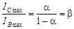
Moreover, the common-emitter circuit permits signal voltage to be amplified as well. Let us connect the load resistor Rl of resistance equal to (for instance) 2000W into the collector circuit, and construct the line of load at the corresponding angle q (Fig. 4.5c). When signal voltage Vinmax = 0.1 V is applied to the input (with the initial bias corresponding to a current of 200m A at a collector to emitter voltage of 5V) an alternating current IBmax of about 100m A appears in the base circuit. Under these conditions the operating point will move up and down along the portion p m q of the load line (i.e. between the static characteristics corresponding approximately to base currents of 300m A and 100m A). The amplitude of output alternating voltage, V OUTmax will run as high as 2V. Hence, voltage gain
 .
.
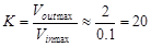
Current gain will differ from its static value, b. For the case considered (Fig. 4.5) it will approximately amount to
 .
.
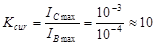
Power gain will equal the product of voltage and current gain, i.e.
 .
.
The advantages of the common-emitter transistor amplifier become clear even from this example, though very approximate and random. In fact, this configuration represents the basic circuit most widely used in transistor amplifying equipment.