2015-08-21
 415
415The input current I1, and output voltage V2 are independent variable components in this system. Thus, functional relations:
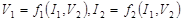 .
.
For low current and voltages:
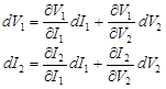 .
.
Let us specify the increments of independent variable components DI1 and DV2 as low harmonic oscillations with complex amplitudes I1 and V2.
The increment of dependent variable components are harmonic oscillations with complex amplitudes V1 and I2. The partial derivatives, standing in front of the independent variable component, are denoted by symbols: h11, h12, h21, h22. So, the equation of the four-terminal network takes on the following form:
V1= h11 I1+ h12V2; I2 = h21 I1+ h22 V2.
From this it follows the physical meaning and the name of h-parameters are:
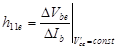
 - the transistor input resistance when the output is short circuited for the variable component of current;
 - the feedback voltage factor when the input is open-circuited for the variable component of current;
 -the differential gain current;
 - the transistor input conductivity when the input is open circuited for a variable component of current.
H–system is a mixed one because its parameters have differ in unlike dimension. The above equations correspond to the transistor circuit shown in Fig.4.7a.
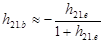
The transistor parameter values depend on its connection diagram (index marks b,e,c.)
In transistor handbooks low frequency parameters are given in the h-system.
The low frequency parameters in a given operative point can be found by using input and output transistor characteristics. The input parameters h11 and h12 can be determined from the transistor input characteristics (Fig. 4.8 a).
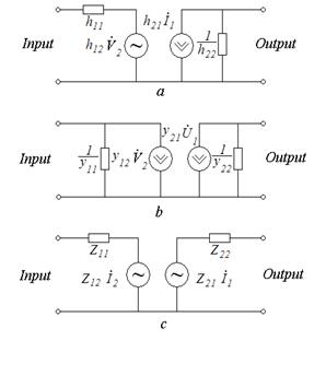
Fig. 4.7. Formal equivalent transistor circuit for: a - H-parameters system, b – Y-parameters system, c - Z-parameters system
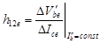
The point A is chosen as a stationary point of the transistor with a common-emitter connection.
Let us take the increment of base current DIb symmetrically with reference to point A at the constant collector voltage Vce (points 1 and 2 Fig. 4.8 a).
 |
Further, we shell find the voltage change DVbe which corresponds to the DIb. Then, the transistor input resistance is:
 .
.
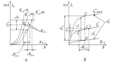
Fig. 4.8. Definition of h-parameters for the circuit with common-emitter connection: a – using input characteristics, b – using output characteristics
The increment of the collector voltage D Uce= D U¢ce – U¢¢ce (points A and B). It is given for constant base current in the operating point I b¢¢. Then, it is possible to defin change of the base voltage D Ube which corresponds to the increment of the collector voltage. So, the feedback voltage factor is:
 .
.
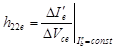
The parameters h 22 and h 21 can be determined from the transistor output characteristics for the same point A (Fig. 4.8b).
Let us give the increment of the collector voltage D Vce (points 3 and 4) symmetrically with reference to the point A at the constant base current I²b, and we can find the current increment D I¢k corresponding to the D Vce.
Then the transistor output conductivity is
 .
.
It is positive because voltage grows with current. Further, we give the increment of the base current D I¢b symmetrically with reference to the point A (point C and D) at the constant collector voltage and find the increment of the collector current D I²e. Then the differential gain base current is:
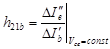 .
.
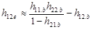
Similarly, it is possible to define transistor parameters for other connection diagrams from corresponding characteristics.
Have in mind, that the transistor parameters of other connection diagrams relate to each other, and you can always switch from one parameter system to another one with the passage formulas (See Table 4.1).
Table 4.1
| Circuit with CE | Circuit with CC | Circuit with CB |

|


|

|


|


|

|