2015-08-21
 478
478Diode thyristors are the simplest semiconductor devices of the given type. The thyristor switching from OFF condition to ON condition takes place when the applied forward voltage exceeds the value of ON-voltage VON
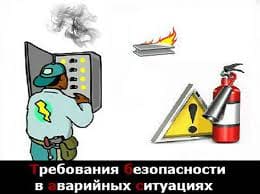
The structure of diode thyristors (Fig.6.1) consists of four semiconductor bands, which have different types of conduction. 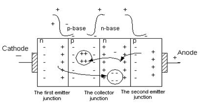
Fig.6.1. Structure of a diode thyristor
The diode thyristor (or dynistor) has three rectifying junctions and two ohmic junctions. The ohmic junction adjacent to the p-type band is called an anode. The other one is called a cathode. When the forward voltage is applied to a dynistor, two margin p-n junctions are biased in forward direction, so they are called emitter junctions. The middle p-n junction is biased in a reverse direction, and it is called a collector junction. Since there is a high potential barrier in the middle of the structure, the current doesn’t flow through a device. At the same time, excess concentration of holes appears in the p-base region. These holes surmount easily the low potential barrier of the second emitter junction and get the n-base region since p-base region has a high negative potential, and then its electric field draws holes into the p-base region. The excess concentration of electrons arises in a similar way in the n-base region.When the forward voltage increases, the current flowing through a dynistar doesn’t increase, but the concentration of excess charge carriers increases in the p- and n-base regions.
At the moment when forward voltage reaches the value of the ON-voltage VON, excess charge carriers compensate completely the potential barrier of the collector junction in p and n-base regions. After that, avalanche process happens and the dynistor opens. The current starts to increase abruptly.
The dynistor will keep ON condition until the flowing current holds excess charge in bases and is sufficient to keep the collector junction in a forward biased position. If the forward current flowing through the device decreases and becomes less than the value of the hold on current Ihld , the dynistor will get OFF condition.
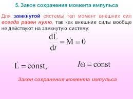
So, the dynistor can get two stable conditions: opened and closed. Let’s consider the CVC of a dynistor shown on Fig.6.2.
The CVC segment between the zero point and point “a”corresponds to dynistor OFF condition. The point ‘a’ is ON point and the voltage applied to dynistor is maximum. The dynistor differential resistance is equal to zero at point ‘a’. When the dynistor is closed (OFF condition), a high voltage is applied to it, but the current remains low. On the “ab” segment CVC has a negative resistance, since current increases with voltage decreases. Flowing current is limited just by the load current and EMF of a power supply. The “cd” segment is a working segment of CVC. When the flowing current reaches the value less than the hold on current, the dynistor gets OFF condition.
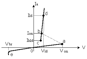
Fig.6.2. Current-voltage characteristic of a dynistor
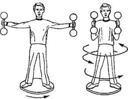
At the reverse voltage a negative potential is applied to the anode, dynistor CVC looks like a common diode one. If the reverse voltage exceeds the brake-down voltage, the dynistor will be destroyed. As a rule, the limit applied voltage must be two times less than the brake-down voltage. The connection diagram of a diode thyristor is shown on Fig.6.3.
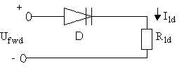
Fig. 6.3. The diode thyristor with an active load