2017-10-31
 220
220 Electronic Engineering 121
Supplementary Reading

 1. Manufacturing the Microchip


The manufacture of microchips can be broken down into seven steps. These include silicon conversion, wafer fabrication, final cleaning, etching, layering, ion implantation, and all final steps leading up to the packaging of the microchip.

Silicon Conversion

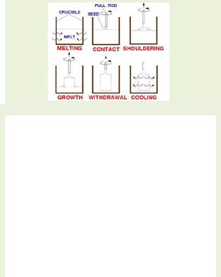
Raw silicon dioxide is heated to be transformed into MGS (metallurgical grade silicon) and then EGS (electronic grade silicon) to reduce the impurity count to one impurity per billion particles. Once the silicon has reached an acceptable purity level, it is grown into a silicon ingot, or a large cylinder which is grown by exposing a small seed of purified silicon to a molten bath of silicon, reaching 1500 – 2000o C. Once the ingot has reached the desired size, it is processed into wafers.
Wafer Fabrication
The large ingot is placed under X-ray observation to check for any impurities created in the silicon conversion process. The ingot is then sliced into wafers as thin as 20 thousandths of an inch with a diamond wire saw. The wafers are tested, constantly checking for uniform flatness, resistance, thickness, and width, then lapped with aluminum slurry to improve surface flatness to +/- 3 microns and polished to be shipped to the wafer fabrication plant.
Fabrication Plant
The wafer fabrication plant is where the wafers are converted from the raw silicon wafer to a computerized microchip. The fabrication plant is a very sterile environment to prevent contamination of the silicon wafers. If only a few particles get on the silicon wafers in the manufacturing process, the wafer is ruined and unusable.
Final Cleaning
An electronic film is placed on the wafer and bathed in a combination of complex chemical acids to remove any minute contaminants. Then, in metallization, an insulating layer is placed on the silicon wafer, and microscopic pieces of metal are sputtered over the insulating layer. Next, gas flows over the insulating layer, diffusing any impurities and

annealing the impurities back to a monocrystalline form.

Etching

The surface of the wafer is coated with photoresist and undergoes a process called photolithography. This is where a mask is placed over the wafer, allowing ultraviolet light to reach the wafer where it is exposed creating there a gooey surface of photoresist. Thus each layer of the microprocessor will have its own mask with a different pattern on it. The next step is to dip the wafer into a bath of developer to remove the photoresist. So a pattern emerges, showing where the mask was on the silicon wafer. The wafer is then dipped into an acid bath, which triggers the chemical etching of the exposed silicon dioxide, creating an intricate pattern on the wafer. The rest of the photoresist is removed, leaving ridges of silicon dioxide on the wafer.
Layering
Since microprocessors require many intricate designs, more layers have to be etched onto the silicon wafer to accommodate the microchip electronic makeup. To start the creation of another layer, a much thinner layer of silicon dioxide is grown over the small ridges and areas etched on the wafer. Next, a layer of polysilicon and photoresist are applied. Then, it is exposed to UV light, once again, creating another pattern on the new photoresist layer. The wafer is bathed in the developer again to expose the polysilicon and silicon dioxide that will eventually be etched away by the acid bath. The photoresist that is still on the wafer is then removed, leaving another layer of ridges of polysilicon and silicon dioxide.
Ion Implantation
The next step, called ion implantation, is a process in which the wafer is bombarded by a stream of ions through an ion implanter with precise targets to alter the silicon conductivity, which is crucial in the microchip functionality. After the implantation of the ions occur on this layer, the next layer is created by repeating the steps described in the preceding two paragraphs. Then, atoms of metal are deposited in between the layers, creating electrical connections between the layers. This entire process is then replicated creating a three dimensional circuitry flowing throughout the wafer.

Because the majority of these processes are automated and controlled tightly by computers, many microchips are built on a single wafer. Each microchip needs to be tested and then cut apart from the other microchips on the same wafer.

http://www.bsu.edu