2018-01-08
 880
880Start here
1. Part of this text is missing. Complete the sentences 1 – 10 with the phrases A – J. Use the information from the text about the types of semiconductors to help you. Put the verb “To be” in brackets in the correct form.
1) There (to be) ……………
2) Intrinsic semiconductors ………….
3) They (to be) ………………
4) Doping (to be) ……………
5) Extrinsic semiconductors ………………
6) Dopant (to be) ……………….
7) The materials chosen as suitable dopants …………
8) Dopants that produce the desired controlled changes (to be)
9) N-type semiconductors (to be) ……………
10) P-type semiconductors (to be) ……………
A. doped with acceptor impurities.
B. the process of deliberately introducing other elements into a crystal.
C. intrinsic and extrinsic semiconductors.
D. have good conductivity.
E. generally insulators.
F. the element introduced by doping.
G. classified as either electron acceptors or donors.
H. doped with donor impurities.
I. do not conduct electric current.
J. depend on the atomic properties of both the dopant and the material to be doped.
2. Find the synonyms to the adjectives: intrinsic and extrinsic.
Reading
3. Match the pictures in Fig. 1.4 with the descriptions 1-3.
Fig. 1.4. Crystal lattices of undoped (pure) and doped (p-type, n-type) semiconductors.
1) 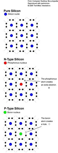 It is an extrinsic semiconductor which is obtained by doping the impurity atoms of the V group in the periodic table of elements. The impurity atoms added, provide extra electrons in the structure and are called donor atoms. The electrons are majority carriers and holes are minority carriers.
2) Each circle represents a silicon atom, and the lines between the atoms represent the shared electrons. Each of the four valence electrons in each silicon atom is shared with one neighboring silicon atom. Thus, each silicon atom is bonded with four other silicon atoms.
3) It is an extrinsic semiconductor which is obtained by doping the impurity atoms of the III group in the periodic table. The impurity atoms added, create holes in the structure and are called acceptor atoms. The holes are majority carriers and electrons are minority carriers.
Listening
4. Listen to the text and do the tasks below.
When voltage is applied to either an N-type or a P-type semiconductor, current flows, for the same reason that it flows in a regular conductor. The negative side of the voltage pushes electrons, and the positive side pulls them. The result is that the random electron and hole movement that's always present in a semiconductor becomes organized in one direction, creating measurable electric current.
Holes move more slowly than electrons. When electrons move in one direction, holes move in the opposite direction. This is like cars parked along a street. If one car moves to an empty slot, the empty slot moves the other way. The cars move to the right, the empty slot to the left. A solitary electron in the presence of a solitary hole will recombine. Only electrons and holes which are free, and hence have not recombined, play a role in electrical conduction.
Even in a highly doped p-type semiconductor there will always be some free electrons. Similarly, n-type semiconductors always contain some holes. The predominant mobile charge carriers are called majority carriers, whilst those in the minority are called minority carriers. For example, the majority carriers in n-type material are free electrons.
5. Study the energy band structures of intrinsic and extrinsic semiconductors in Fig. 1.5.
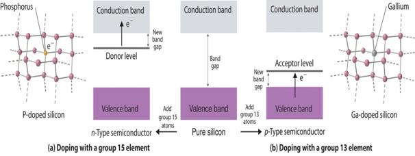
Fig. 1.5. Energy band structures of undoped (pure) and doped (n-type, p-type) semiconductors.
6. Make a comparative table of an N-type and a P-type semiconductor. Use the information in the previous tasks.
Types of extrinsic semiconductors
| N-type semiconductor | P-type semiconductor | |
| Majority charge carriers | ||
| Minority charge carriers | ||
| Group of the impurity atoms in the periodic table of elements | ||
| Impurities are called | ||
| Extra energy level | ||
| Fermi level lies in between | ||
Vocabulary
7. Use the example of a word map in Fig. 1.6 to make your own word maps of the following words:
1) semiconductor
2) doping
3) impurity
4) hole
5) electron
6) conductivity
7) crystal
The Plan of a Word Map:
1) Vocabulary word
2) Sentence or phrase from the text
3) The matching dictionary definition
4) Synonym
5) Antonym
6) Other forms of the word
7) Your association, example or sketch
8) Your own sentence
Fig. 1.6. Word map
Review
8. Make a concept map on the topic: “Semiconductors.”
A concept map is a visual organizer that can enrich your understanding of a new concept. It is a way to display how your mind "sees" a particular topic. Using a graphic organizer, think about the concept in several ways. By constructing a concept map, you reflect on what you know and what you don't know.
There are several ways to construct concept maps. Most include the following steps:
1) Model how to identify the major ideas or concepts.
2) Organize the ideas into categories. Your organization may change as you continue to read and add more information.
3) Use lines or arrows on the map to represent how ideas are connected to one another. Limit the amount of information on the map to avoid frustration.
4) Share and reflect on how you made the connections between concepts.
5) Use the concept map to summarize what was read.
UNIT 2
DIODE
Fig. 2.1. Diodes
Contents
Ø What is a Diode?
Ø Creating a P-N Junction.
Ø Types of Diodes.
Ø Diode Applications.
WHAT IS A DIODE?
Warm up
1. Revise your vocabulary on the topic: “Semiconductors” with the word association game.
Procedure:
The students associate the teacher’s chosen word: “Semiconductor”. Ask all the students to stand up. The first player will say any word associated with the chosen one. This continues from player to player. If a student says a disassociated word, repeats a word or is too slow to answer, he is out and has to sit down. The winner is the last person left standing. All associated words must be written on the blackboard.
2. Revise the verb “To be” and the concept of semiconductors making your own sentences.
Procedure:
You will need a ball, but a screwed up piece of paper is fine. The teacher throws the ball to one student and says a sentence such as: “Silicon and germanium are semiconductor materials.” The student must reply with a sentence on this topic using the verb “to be”. When answered the ball is thrown to the next student, who continues. The teacher says the last sentence: “Semiconductors are widely used in Diodes”.
3. Answer the following questions:
How much do you know about diodes?
Have you ever heard about diodes?
What do you think they are?
How do they work?
Listening
4. Listen to the text and use the information in Fig. 2.2 to help your comprehension.
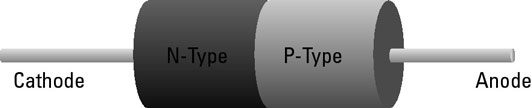
Fig. 2.2 Internal structure of a p-n diode.
Move over bulbs: there are better ways to make light now! There are those compact fluorescent lamps, for example – the ones that save your energy and money. But, even better, there are light-emitting diodes (LEDs) that are just as bright as bulbs, last virtually forever, and use hardly any energy at all. Diodes have been around for many decades. Let's take a closer look at them!
A diode is an electronic component made from a combination of a P-type and N-type semiconductor material, known as a p-n junction, with leads attached to the two ends. These leads allow you to easily incorporate the diode into your electronic circuits.
The lead attached to the n-type semiconductor is called the cathode. Thus, the cathode is the negative side of the diode. The positive side of the diode – that is, the lead attached to the p-type semiconductor – is called the anode.
When a voltage source is connected to a diode such that the positive side of the voltage source is on the anode and the negative side is on the cathode, the diode becomes a conductor and allows current to flow. Voltage connected to the diode in this direction is called forward bias.
But if you reverse the voltage direction, applying the positive side to the cathode and the negative side to the anode, current doesn't flow. In effect, the diode becomes an insulator. Voltage connected to the diode in this direction is called reverse bias.
5. Listen to the text once more and decide if the sentences are true or false.
1. Bulbs save energy and money.
2. A diode is an electronic component made from a p-n junction.
3. The cathode is the negative side of the diode.
4. The positive side of a diode is called the anode.
5. The lead attached to the p-type semiconductor is called the cathode.
6. The lead attached to the n-type semiconductor is called the anode.
7. Forward bias doesn't allow current to flow.
8. Reverse bias allows current to flow through the diode.
Reading
6. Read the text and answer the questions:
Where is the anode?
Where is the cathode?
Indicate the anode and cathode in Figure 3.
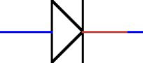 Fig. 2.3. Electronic symbol of a diode.
The schematic symbol of a diode is shown in Fig. 2.3. Here are two useful tricks for remembering which side of the symbol is the anode and which is the cathode:
· think of the anode side of the symbol as an arrow that indicates the direction of conventional current flow – from positive to negative. Thus, the diode allows current to flow in the direction of the arrow;
· think of the vertical line on the cathode side as a giant minus sign, indicating which side of the diode is negative for forward bias.
7. Read the text and fill in the gaps with the words and word combinations in the box.
| backward reverse biased amount peak inverse voltage forward voltage drop diode current forward biased |
Forward and reverse bias can be illustrated with two very simple circuits that connect a lamp to a battery with diodes. In the circuit on the left (Fig. 2.4), the diode is (1) ………………., so current flows through the circuit and the lamp lights up. In the circuit on the right, the diode is (2) ……………, so current doesn't flow and the lamp remains dark.
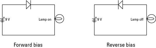
Fig. 2.4 Forward biased and reverse biased circuits.
Note that in a typical diode, a certain amount of forward voltage is required before any current will flow. This (3) …………..is usually very small. In most diodes, this voltage is around half a volt. Up to this voltage, current doesn't flow. However once the forward voltage is reached, current flows easily through the (4)….............
This minimum threshold of voltage in the forward direction is called the diode's forward voltage drop. That's because the circuit loses this voltage at the diode. For example, if you were to place a voltmeter across the leads of the diode in the forward-biased circuit, you would read the (5) …………………of the diode.
Diodes also have a maximum reverse voltage they can withstand before they break down and allow current to flow (6) ……………….through the diode. This reverse voltage (sometimes called PIV, for (7) ………………, or PRV for peak reverse voltage) is an important specification for diodes you use in your circuits, as you need to ensure that your diodes won't be exposed to more than their PIV rating.
Besides the forward-voltage drop and peak inverse voltage, diodes are also rated for a maximum current rating. Exceed this (8) ………………, and the diode will be damaged beyond repair.
Vocabulary
8. Choose the correct spelling of these words and translate them:
| diode diod | p-n juction p-n junction | anod anode | foward bais forward bias | reverse voltage revers voltag |
| cathode catode | curent ratin current rating | lead laed | cercuit circuit | threshold treshold |
Speaking
9. Work in pairs, choose one of the following questions and discuss it.
1) What is the connection between diodes and semiconductors?
2) How would you assess the importance of diodes?
3) Are vacuum tube diodes still used or are they totally replaced by semiconductors?